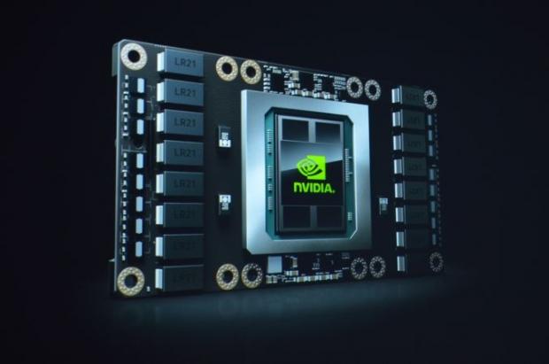
Today at their 2016 GPU Technology Conference, NVIDIA announced the first of their Pascal architecture powered Tesla cards, the Tesla P100.
The P100 is the first major update to the Tesla HPC family since the launch of the first Kepler cards in late 2012. This does represent a very big performance increase as far as the Tesla family is concerned, as it combines the smaller 16nm manufacturing process and the Pascal architecture.
Powering the Tesla P100 is a partially disabled version of NVIDIA’s new GP100 GPU, with 56 of 60 SMs enabled. The GP100 is truly a monster, there is no other way of describing the power of the component. It measures at 610mm2 in die size on TSMC’s 16nm FinFET process and composed of 15.3B transistors.
GP100 is being produced on TSMC’s Chip-On-Wafer-On-Substrate technology, with this line apparently being used for putting the GPU and HBM2 DRAM stacks on the same interposer.

We will surely get back to the complete details of the Pascal technology at a later time, however, at present, the thing that is worth noticing is the fact that Pascal here is 64 FP32 CUDA cores per SM, versus 128 on Maxwell.
Each of those SMs also contains 32 FP64 CUDA cores, giving us the 1/2 rate for FP64 and new to the Pascal architecture is the ability to pack 2 FP16 operations inside a single FP32 CUDA core, when under the right conditions.
The GP100 features 1.48GHz of boost clock, which is capable of offering 10.6 TFLOPS of FP32 performance or 5.3 TFLOPS of FP64 performance.
Paired with the GP100 GPU on Tesla P100 is 16GB of HBM2 VRAM, which is divided out into 4 stacks for a 4096-bit memory bus. NVIDIA says that the P100 offers 720GB/sec of memory bandwidth, which works out to a memory clock of 1.4Gbps.
The TDP of the GPU is 300W, so it definitely much higher than the previous generations which were mostly in the 230W-250W range.


